[GUEST ACCESS MODE: Data is scrambled or limited to provide examples. Make requests using your API key to unlock full data. Check https://lunarcrush.ai/auth for authentication information.]  Jukan [@Jukanlosreve](/creator/twitter/Jukanlosreve) on x 22.6K followers Created: 2025-07-22 07:03:10 UTC Report: Samsung Electronics Considers Adopting Hybrid Bonding for 'HBM4E 16-Hi'... Sample Evaluation Underway Samsung Electronics has announced its plan to apply hybrid bonding technology starting with HBM4E (7th generation high-bandwidth memory) 16-layer, at the earliest. Sample testing is currently in progress, and business feasibility and investment costs are expected to be key factors for commercialization. Kim Dae-woo, Senior Vice President at Samsung Electronics, introduced the packaging technology roadmap for next-generation semiconductors at the '2025 Commercial Semiconductor Development Technology Workshop' on the 22nd. HBM is a memory that enhances data processing performance by vertically stacking multiple DRAMs and connecting them with TSV (Through-Silicon Via). Traditional HBM manufacturing methods have used a thermo-compression (TC) bonding approach, inserting tiny bumps between each DRAM. However, as the number of stacked DRAM layers in HBM increasingly grows to 16, 20, or more, the application of existing TC bonding is expected to become difficult. This is due to the HBM package thickness being limited to a maximum of XXX micrometers (μm). Analysis suggests that thinning each DRAM further or narrowing the gap between DRAMs also has limitations. For this reason, the industry has been developing hybrid bonding as an alternative technology, which directly attaches the copper interconnects of chips and wafers. This technology offers the advantage of significantly reducing HBM package thickness because it does not use bumps. It also allows for denser integration of I/O (input/output terminals) and improved heat dissipation. However, the adoption timeline for hybrid bonding has been uncertain due to its high technical difficulty and the pressure of increased costs from transitioning investments from existing TC bonding. Samsung Electronics is also understood to be deep in contemplation, as it has not yet finalized a specific adoption timeline for hybrid bonding. According to the roadmap unveiled today, Samsung Electronics plans to introduce hybrid bonding starting with HBM4E (7th generation) at the earliest. To this end, Samsung Electronics is reportedly providing 16-layer HBM samples based on hybrid bonding to customers for evaluation. Senior Vice President Kim explained, "Even with just XX layers of HBM stacking, it becomes difficult to manage heat, so we are preparing to gradually implement hybrid bonding from that point. Whether hybrid bonding will be commercialized in HBM4E depends on market considerations and investment costs." Samsung is also preparing for the custom HBM business, for which demand is expected to increase in the future. Currently, multiple global big tech companies such as Google, Nvidia, and AMD are demanding HBMs with performance tailored to their AI semiconductors. Senior Vice President Kim stated, "We are receiving many inquiries for custom HBMs, and we are preparing to create Samsung Electronics' unique custom HBMs, such as by incorporating computational functions into the base die." 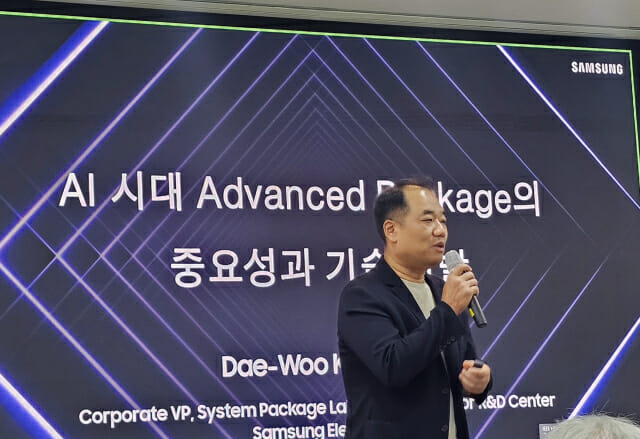 XXXXXX engagements  **Related Topics** [hybrid](/topic/hybrid) [investment](/topic/investment) [stocks technology](/topic/stocks-technology) [underway](/topic/underway) [$ssnlf](/topic/$ssnlf) [$005930ks](/topic/$005930ks) [samsung](/topic/samsung) [Post Link](https://x.com/Jukanlosreve/status/1947552987913851034)
[GUEST ACCESS MODE: Data is scrambled or limited to provide examples. Make requests using your API key to unlock full data. Check https://lunarcrush.ai/auth for authentication information.]
 Jukan @Jukanlosreve on x 22.6K followers
Created: 2025-07-22 07:03:10 UTC
Jukan @Jukanlosreve on x 22.6K followers
Created: 2025-07-22 07:03:10 UTC
Report: Samsung Electronics Considers Adopting Hybrid Bonding for 'HBM4E 16-Hi'... Sample Evaluation Underway
Samsung Electronics has announced its plan to apply hybrid bonding technology starting with HBM4E (7th generation high-bandwidth memory) 16-layer, at the earliest. Sample testing is currently in progress, and business feasibility and investment costs are expected to be key factors for commercialization.
Kim Dae-woo, Senior Vice President at Samsung Electronics, introduced the packaging technology roadmap for next-generation semiconductors at the '2025 Commercial Semiconductor Development Technology Workshop' on the 22nd. HBM is a memory that enhances data processing performance by vertically stacking multiple DRAMs and connecting them with TSV (Through-Silicon Via). Traditional HBM manufacturing methods have used a thermo-compression (TC) bonding approach, inserting tiny bumps between each DRAM.
However, as the number of stacked DRAM layers in HBM increasingly grows to 16, 20, or more, the application of existing TC bonding is expected to become difficult. This is due to the HBM package thickness being limited to a maximum of XXX micrometers (μm). Analysis suggests that thinning each DRAM further or narrowing the gap between DRAMs also has limitations. For this reason, the industry has been developing hybrid bonding as an alternative technology, which directly attaches the copper interconnects of chips and wafers. This technology offers the advantage of significantly reducing HBM package thickness because it does not use bumps. It also allows for denser integration of I/O (input/output terminals) and improved heat dissipation. However, the adoption timeline for hybrid bonding has been uncertain due to its high technical difficulty and the pressure of increased costs from transitioning investments from existing TC bonding. Samsung Electronics is also understood to be deep in contemplation, as it has not yet finalized a specific adoption timeline for hybrid bonding.
According to the roadmap unveiled today, Samsung Electronics plans to introduce hybrid bonding starting with HBM4E (7th generation) at the earliest. To this end, Samsung Electronics is reportedly providing 16-layer HBM samples based on hybrid bonding to customers for evaluation.
Senior Vice President Kim explained, "Even with just XX layers of HBM stacking, it becomes difficult to manage heat, so we are preparing to gradually implement hybrid bonding from that point. Whether hybrid bonding will be commercialized in HBM4E depends on market considerations and investment costs." Samsung is also preparing for the custom HBM business, for which demand is expected to increase in the future. Currently, multiple global big tech companies such as Google, Nvidia, and AMD are demanding HBMs with performance tailored to their AI semiconductors.
Senior Vice President Kim stated, "We are receiving many inquiries for custom HBMs, and we are preparing to create Samsung Electronics' unique custom HBMs, such as by incorporating computational functions into the base die."

XXXXXX engagements

Related Topics hybrid investment stocks technology underway $ssnlf $005930ks samsung