[GUEST ACCESS MODE: Data is scrambled or limited to provide examples. Make requests using your API key to unlock full data. Check https://lunarcrush.ai/auth for authentication information.]  Jukan [@Jukanlosreve](/creator/twitter/Jukanlosreve) on x 22.6K followers Created: 2025-07-21 23:30:34 UTC Report: “Vertical and Planar ‘Two‑Track’ Approach”… Samsung Electronics’ Next‑Generation DRAM Development Strategy Revealed Samsung Electronics plans to introduce the X nm‑class DRAM currently under development for commercialization within three years with a ‘4F²’ DRAM cell structure—changing the DRAM layout from planar to vertical—while simultaneously advancing development of the existing planar 6F²‑structured X nm‑class DRAM. Moving to a vertical DRAM structure raises design complexity and requires significant changes in the manufacturing process, driving up production costs; this two‑track strategy is reportedly aimed at reducing costs and securing development time for the 4F² structure. Samsung Electronics intends to apply the 4F² cell structure starting with the X nm (0a) DRAM, the generation following the XX nm‑class sixth generation (1c, roughly 11–12 nm) DRAM slated for mass production in the second half of this year. DRAM stores data in cells, the basic unit capable of holding a single digital bit. The area occupied by one cell is expressed as F². To date, the standard cell has been a planar 6F² layout, with three vertical bitlines and two horizontal wordlines. However, below the XX nm process node, planar structures face miniaturization limits; to both shrink DRAM size and increase density, Samsung is developing a 4F² DRAM that reduces each line to two and arranges the transistor—responsible for DRAM switching—in a vertical configuration. Industry sources report that Samsung Electronics is preparing not only the 4F² structure but also further development of the existing 6F² DRAM for its X nm (0a) generation. TechInsights Senior Vice President Choi Jeong‑dong explained, “Mass‑producing 4F² DRAM in a vertical structure entails major changes in design, process, and manufacturing equipment. By also advancing the existing planar process one generation further, only circuit linewidth needs to be reduced without redesigning or retooling, buying additional development time for 4F² DRAM—so we are evaluating that possibility.” With each DRAM generation, finer process technologies narrow circuit linewidths, reducing chip size and boosting density to enhance performance and power efficiency. Currently, Samsung Electronics, SK Hynix, and Micron compete with their fourth (1a) and fifth (1b) generation XX nm‑class DRAM as flagship products, and plan to begin full‑scale production of sixth generation XX nm‑class (1c) DRAM in the second half of this year. However, below the XX nm node, manufacturing difficulty and costs soar, making structural changes in DRAM inevitable. For this reason, memory vendors have chosen to switch from planar to vertical structures to improve performance and power efficiency. Samsung plans to adopt the 4F² structure in the generation following its seventh generation XX nm‑class (1d) DRAM product, while SK Hynix is scheduled to introduce its 4F² DRAM one generation later. Since Samsung is developing the technology one generation ahead of SK Hynix, it is reportedly keeping all options open and continuously evaluating possibilities. A semiconductor industry insider noted, “One approach is to develop the 0a generation at roughly XXX nm using the existing 6F² structure, then switch to a XXX nm process with a 4F² structure in the following generation. The final decision will be made through development and evaluation.” Sources indicate that Samsung plans to complete development and supply samples of the product to customers as early as 2027, aiming for mass production within three years. An industry insider commented, “Internally, there is a strong sense of urgency at Samsung because it has failed to gain an edge over SK Hynix since the fourth‑generation (1a) XX nm‑class DRAM. For next‑generation DRAM, Samsung is establishing a multifaceted development roadmap to widen its lead in the DRAM market.” 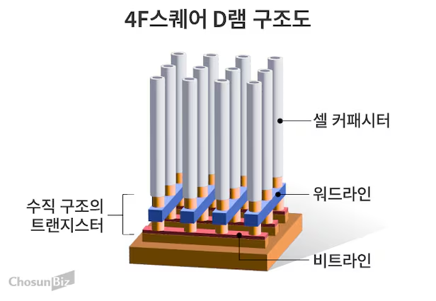 XXXXX engagements  **Related Topics** [dram](/topic/dram) [electronics](/topic/electronics) [$ssnlf](/topic/$ssnlf) [$005930ks](/topic/$005930ks) [samsung](/topic/samsung) [Post Link](https://x.com/Jukanlosreve/status/1947439086652035539)
[GUEST ACCESS MODE: Data is scrambled or limited to provide examples. Make requests using your API key to unlock full data. Check https://lunarcrush.ai/auth for authentication information.]
 Jukan @Jukanlosreve on x 22.6K followers
Created: 2025-07-21 23:30:34 UTC
Jukan @Jukanlosreve on x 22.6K followers
Created: 2025-07-21 23:30:34 UTC
Report: “Vertical and Planar ‘Two‑Track’ Approach”… Samsung Electronics’ Next‑Generation DRAM Development Strategy Revealed
Samsung Electronics plans to introduce the X nm‑class DRAM currently under development for commercialization within three years with a ‘4F²’ DRAM cell structure—changing the DRAM layout from planar to vertical—while simultaneously advancing development of the existing planar 6F²‑structured X nm‑class DRAM. Moving to a vertical DRAM structure raises design complexity and requires significant changes in the manufacturing process, driving up production costs; this two‑track strategy is reportedly aimed at reducing costs and securing development time for the 4F² structure. Samsung Electronics intends to apply the 4F² cell structure starting with the X nm (0a) DRAM, the generation following the XX nm‑class sixth generation (1c, roughly 11–12 nm) DRAM slated for mass production in the second half of this year.
DRAM stores data in cells, the basic unit capable of holding a single digital bit. The area occupied by one cell is expressed as F². To date, the standard cell has been a planar 6F² layout, with three vertical bitlines and two horizontal wordlines. However, below the XX nm process node, planar structures face miniaturization limits; to both shrink DRAM size and increase density, Samsung is developing a 4F² DRAM that reduces each line to two and arranges the transistor—responsible for DRAM switching—in a vertical configuration.
Industry sources report that Samsung Electronics is preparing not only the 4F² structure but also further development of the existing 6F² DRAM for its X nm (0a) generation. TechInsights Senior Vice President Choi Jeong‑dong explained, “Mass‑producing 4F² DRAM in a vertical structure entails major changes in design, process, and manufacturing equipment. By also advancing the existing planar process one generation further, only circuit linewidth needs to be reduced without redesigning or retooling, buying additional development time for 4F² DRAM—so we are evaluating that possibility.”
With each DRAM generation, finer process technologies narrow circuit linewidths, reducing chip size and boosting density to enhance performance and power efficiency. Currently, Samsung Electronics, SK Hynix, and Micron compete with their fourth (1a) and fifth (1b) generation XX nm‑class DRAM as flagship products, and plan to begin full‑scale production of sixth generation XX nm‑class (1c) DRAM in the second half of this year.
However, below the XX nm node, manufacturing difficulty and costs soar, making structural changes in DRAM inevitable. For this reason, memory vendors have chosen to switch from planar to vertical structures to improve performance and power efficiency. Samsung plans to adopt the 4F² structure in the generation following its seventh generation XX nm‑class (1d) DRAM product, while SK Hynix is scheduled to introduce its 4F² DRAM one generation later. Since Samsung is developing the technology one generation ahead of SK Hynix, it is reportedly keeping all options open and continuously evaluating possibilities.
A semiconductor industry insider noted, “One approach is to develop the 0a generation at roughly XXX nm using the existing 6F² structure, then switch to a XXX nm process with a 4F² structure in the following generation. The final decision will be made through development and evaluation.”
Sources indicate that Samsung plans to complete development and supply samples of the product to customers as early as 2027, aiming for mass production within three years. An industry insider commented, “Internally, there is a strong sense of urgency at Samsung because it has failed to gain an edge over SK Hynix since the fourth‑generation (1a) XX nm‑class DRAM. For next‑generation DRAM, Samsung is establishing a multifaceted development roadmap to widen its lead in the DRAM market.”

XXXXX engagements

Related Topics dram electronics $ssnlf $005930ks samsung